

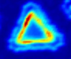
Photo caption: Photoluminescence intensity map shows a typical piece of the lateral heterostructures
A team at the UW Clean Energy Institute (CEI) is developing ways to connect two-dimentional sheets of solar collector material, one atom thick, that have the potential to be as flexible and foldable as a piece of paper and as strong as any material that exists on earth. This team of physics faculty and student researchers are creating the building blocks upon which the next generation of solar materials and energy storage devices could be created.
UW Physics faculty Xiaodong Xu and David Cobden, along with CEI graduate fellow Sanfeng Wu, work in the fast-growing research field of 2D materials. It is a very new field which isolates and studies the characteristics of single sheets of atomically thin material. These single-layer materials, also known as monolayers, are flexible and act as semiconductors with extraordinary electronic properties. Semiconductors are an essential component in all modern solar cells and electronics.
The UW team and collaborators recently demonstrated how to grow different monolayer semiconductors so they are connected edge to edge seamlessly to form “heterojunctions.” This foundational work is groundbreaking and was published recently in the journal Nature Materials.
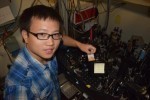
CEI graduate fellow Sanfeng Wu uses lasers to investigate the light-matter interactions of the 2D material.
Xu compares the work to building the first Lego set for 2D materials. “Once you prove that you can connect the single layer of materials, then you can build entire communities to study because there are so many 2D materials. It’s a big family. But we needed to do the foundational work and build a platform from which to study them,” he said.
The work has important implications for creating new types of photovoltaics, batteries, LEDs, lasers and electronic devices. Major new research grants from the U.S. Department of Energy, National Science Foundation, and Department of Defense are allowing the UW team to assemble a global collaboration network that can seize the new opportunities afforded by their breakthrough method for building these new semiconducting connections. Read more here:
Scientists craft a semiconductor junction only three atoms thick