
Graduate Student, Chemical Engineering
Thin-Film Vapor-Liquid Solid Growth of GaAs for Low-Cost High Efficiency Photovoltaics
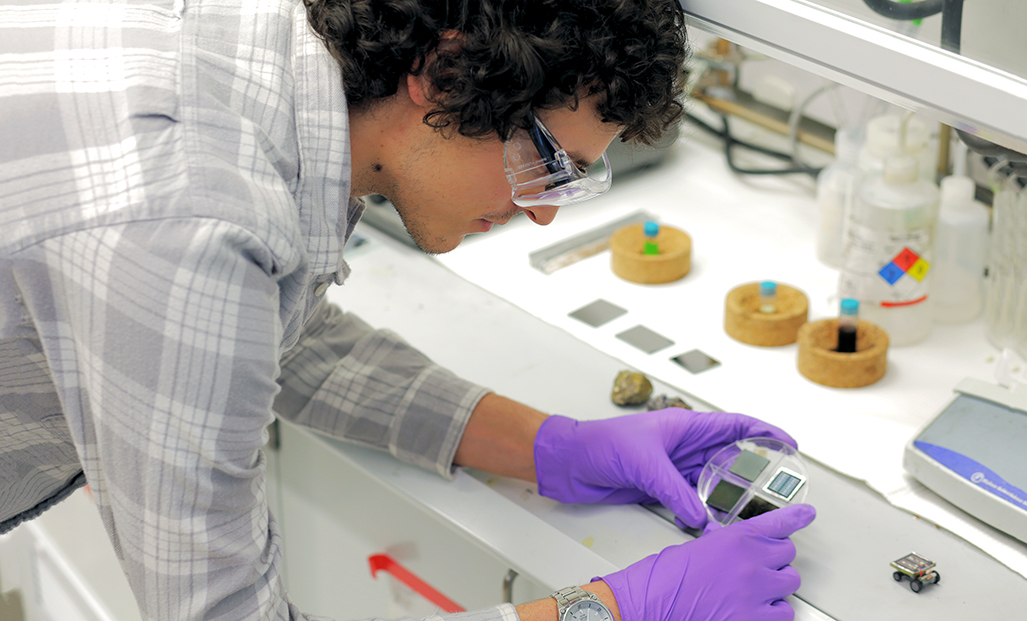
The best photovoltaic material known to humankind is GaAs. It’s bandgap is perfectly matched to the spectrum, and it holds the world record for single junction power conversion efficiency at 28.8%. The starting raw materials (gallium and arsenic) are abundant, cheap, and only weakly demanded for other applications. Despite this, current start-of-the-art GaAs solar cells cost over $8/W. The problem is the processing cost. GaAs cells are grown using metal-organic chemical vapor deposition (MOCVD) on single crystal GaAs wafers and then lifted off. MOCVD has a low materials utilization rate and requires expensive, highly toxic, and dangerous pyrophoric precursors such as trimethyl gallium and arsine gas (AsH3). However, if high quality GaAs could be grown using low-cost techniques it would revolutionize the solar energy technology. With a key recent advance in vapor-liquid-solid (VLS) growth techniques, this may be possible. Recently, the Javey group at Berkeley used a new VLS technique to grow thin films (3 μm thick) of InP with single crystal domains on the order of ~ 3 x 100 x 100 μm on low-cost molybdenum substrates. The materials had remarkable near-wafer optoelectronic quality (quasi Fermi level splitting of 0.93 eV, note the bandgap of InP is 1.34 eV). The key technical advance was controlling the nucleation and growth of InP in a phosphorous saturated molten indium layer. Here, we are working to develop a scheme to nucleate and grow high quality GaAs by a thin film VLS method. This exploratory effort has never been attempted (to our knowledge) and may result in a breakthrough for solar energy processing.