
About
The Photonics Research Center is a multi-user shared research facility located in Bagley Hall 453 and 459 that houses state-of-the art equipment for the fabrication, materials characterization, and device testing associated with thin film optoelectronic devices. The primary goal of the center is to facilitate research and development of organic electronic and optoelectronic devices such as thin-film transistors, energy efficient light-emitting diodes, and solar cells. At the core of the facility are two inert atmosphere processing and thin-film deposition systems that allow for sample preparation and device testing without exposing samples to water and oxygen. This capability is essential to making high-performance, durable devices from organic semiconductors, but may be used by other users provided their processes are compatible with the processes of established users. An extensive array of equipment for the optical and electrical characterization of materials and thin film devices is also available for use in and out of the gloveboxes.
Training
The Photonics Research Center operates as a cost center available to graduate students, academic, non-profit, national laboratory, and industrial researchers. To become authorized for a particular piece of equipment, users must undergo one training session and then schedule a follow up session with the instructor, where users demonstrate your knowledge of the system or process. Users that have successfully completed training will be granted key access to the rooms. Only qualified users are allowed 24/7 access to the facility.
Instruments and Rates
| Billable Unit | UW Rate | Commercial Rate |
| Signatone Probe Station | $14.36 | $143.61 |
| Spin Coater Durip Box 2 | $13.09 | $130.91 |
| Spin Coater Murdock Box 2 | $13.09 | $130.91 |
| Evaporators (Durip & Murdock) | $22.18 | $221.82 |
| Nicolet 8700 FTIR | $15.37 | $153.68 |
| Pulsed Laser Diodes | $11.91 | $119.08 |
| Quantum Yield LED System | $18.25 | $182.52 |
| UV/O3 Cleaner | $2.97 | $29.67 |
| Spec E-chem | $12.82 | $128.26 |
Instrument Details
| Instrument | Description |
|---|---|
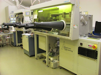 |
Glovebox workstations (MBraun) and thin-film deposition systems (Angstrom Engineering): This system provides inert working conditions for thin-film device preparation and fabrication. It can attain purity levels of less than 1 ppm oxygen and moisture. The workstations integrate thin film deposition systems and components for semiconductor device fabrication applications, including spin coater (Laurell WS-400-6NPP), multi-source thermal deposition and e-beam evaporation (AMOD and EVOVAC from Angstrom Engineering). |
 |
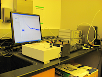
External Quantum Efficiency Measurement System – Integrating Sphere (Hamamatsu, C9920-12): This instrument measures absolute quantum yields of photo-luminescent materials. Both solid (films, powders) and liquid samples can be analyzed. A Xenon lamp coupled to a monochromator enables photo-excitation over a broad spectral range. This system uses a high-sensitivity photonic multi-channel analyzer (Hamamatsu C10027-01) to measure a light emission spectrum. The light flux is then calculated from the spectrum to measure the external quantum efficiency of light emitting materials. |
 |
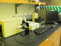
Fluorescence Lifetime Spectrometer (PicoQuant, FluoTime 100, PicoHarp 300): The FluoTime 100 spectrometer allows recording of fluorescence decays by means of Time-Correlated Single Photon Counting (TCSPC). Decay times of down to 40 picoseconds can be resolved. The time resolution of the time correlated single photon counting system (PicoHarp 300) is specified with 4 ps. The laser excitation wavelengths available are: 375, 405, 470, 640 and 750 nm. The laser pulse width is in the range of 70 – 90 ps. The system can be used with films on substrates or solutions. Cut-off filters are available for spectral filtering of the emission light. |
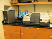 |
Fourier Transform Infrared Spectrometer – (ThermoScientific, Nicolet-8700): FTIR spectrometer with a HgCdTe detector, step-scan capabilities, and a Harrick GATR grazing angle attenuated total reflectance (ATR) accessory. This spectrometer can be used in the ATR geometry to characterize solid, thin film, or liquid samples in the infrared spectral region. |
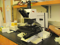 |
Wafer Inspection Microscope (Leica, Reichert Polylite 88): Brightfield microscope (upright, reflected light illumination) with variable magnification of up to 100x. |
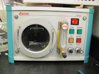 |
Low pressure plasma system (Diener, Femto): This plasma system features a stainless steel plasma chamber with a plasma etching RF driven aluminum or steel electrode. The plasma power supply can be continuously adjusted from 0 – 100 W at 40 kHz. The system can be operated with different gases for cleaning, activation and etching of surfaces. |
Contact
Photonics Center Manager
Department of Chemistry – Ginger Group
Box 351700
Seattle, WA 98195